[pageLogInLogOut]
TRÜTZSCHLER SPINNING - THE NEW CARD

#Industry 4.0 / Digitalization

High-frequency technology entirely in glass

© Endress+Hauser AG - The side view of the glass package shows its three-layered structure, vias, and solder balls.
To remain competitive in the field of the Internet of Things, even medium-sized industrial and process metrology companies need to increasingly integrate their sensor circuits into ASICs (application-specific integrated circuits). The semiconductor industry is currently meeting this need with lower costs for development cycles and decreasing quantity hurdles.

This is not occurring often enough in chip packaging, meaning that ASICs requiring individual packages are at risk of being bogged down due to the quantity hurdles of package service providers, most of which are Asian. This issue is now resolved by a consortium of seven partners from industry and research. 

Radar sensors for industrial and process metrology, as addressed in the project “Glass Interposer Technology for Implementing Highly Compact Electronic Systems for High-frequency Applications” (GlaRA) sponsored by the BMBF (Bundesministerium für Bildung und Forschung, German Federal Ministry of Education and Research), are a good example of the needs profile described above. Standard packages do not work because of the frequencies exceeding 100 GHz – higher than those of mobile communications technology – and the stricter environmental requirements. They must allow for adaptation to specialized sensor ASICs and permit manufacturing in medium-sized quantities at competitive prices.

© Endress+Hauser AG - Conducting paths, ASIC, and waveguide holder can be seen in this view of the package (base area 5.9 x 4.4 mm²).


To this end, the consortium has developed and characterized a reliable interposer technology as a system-in-package (SiP) based on glass for broadband millimeter wave modules that can be used in sensors and communication at frequencies above 100 GHz. The technology platform demonstrated here constitutes a sensor packaging revolution: Compared to the state of the art, it uses various waveguide concepts, high-density micro wiring, and hermetic encapsulation to increase functions able to be integrated. In addition, it makes applications up to 300 GHz possible thanks to high precision and material qualities. This is implemented within a single material system (glass) through excellent waveguide properties and high-precision micromachining, among others.

The use of glass interposers with electric feedthroughs (vias) provides hermetic packaging able to enclose the components between two glass interposers. The packages are manufactured at wafer level with a diameter of up to 300 mm. This allows for moderate costs thanks to the simultaneous processing of many components and alignment accuracy within the narrow tolerances of RF technology. Adapted standard systems originally used for machining silicon wafers are employed for this, greatly accelerating commercial implementation. Glass is also available in large panels, considerably simplifying scaling to large quantities.

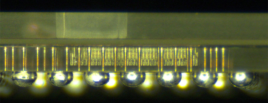
The results represent exceptionally great success for an R&D project sponsored by the BMBF. The consortium demonstrates this with an extremely compact radar front end developed at Endress+Hauser AG for future radar fill level sensors, with an operating frequency of 160 GHz. The glass package is tiny (5.9 x 4.4 x 0.8 mm³) and contains a radar ASIC in SiGe technology, all electrical connections to external electronics, test structures for characterization, and a waveguide connection that can also be used as an integrated primary emitter for a lens antenna. Such future fill level sensors feature high distance resolution, measuring accuracy, and beam focusing at very compact dimensions. Therefore, they are of great interest for the constantly shrinking and increasingly more modular systems of smart process metrology.


The demos were produced using a new kind of process chain, starting with the revolutionary laser-induced deep etching (LIDE) of LPKF Laser & Electronics AG. The process of generating microstructures in glass prevents damage to the material, which is mandatory for a manageable and hermetic glass package. The Fraunhofer Institute for Reliability and Micro-Integration has implemented a process fit for industrial use for metallizing the glass vias with high aspect ratios. A wafer bonding process is used to hermetically package the assembled components by bonding two glass wafers, each of which have vias and cavities.

The conducting paths on the glass substrates are structured and metallized at PacTech GmbH. Using PacTech’s SB² process, a laser-supported process for the sequential build-up of solder balls, solder deposits are placed on contact surfaces produced without         external current. Different alloys are used to enable staggered assembly at different soldering temperatures. MSG Lithoglas GmbH assists with the implementation of the HF packages by producing cavities used to hold the ASIC and other components. In addition, high-precision spacers made of glass are produced by means of low-temperature coating.

With a high-frequency concept developed for the new package by the Institute for Microwave Technology of Ulm University, the radar signal – at more than 100 GHz – can both illuminate a lens directly via a primary beam and be guided at low loss to a detached antenna via a flexible dielectric waveguide. The different options for emitting radar signals from the package enable a great variety of applications. Sentronics Metrology GmbH has developed a 3D high-speed sensor with layer resolutions in the sub-nanometer range for quality control. Among other uses, the sensor has been qualified for detecting leaks in the encapsulated, evacuated glass packages.

© Endress+Hauser AG - A mounted radar sensor with a glass package in the center and an attached dielectric waveguide


The industry partners are very interested in the future commercial availability of the technology, as they see potential for many other areas of application, such as pressure measurement technology, liquid analysis, photonics, MEMS, medical technology, and communication technology beyond 5G.

The “GlaRA” funding project is being sponsored by the BMBF from August 2017 to March 2021 under reference no. 16ES0687K as part of the TechSys call.


More News from Fraunhofer-Institut für Zuverlässigkeit und Mikrointegration IZM

More News on Industry 4.0 / Digitalization

#Dyeing, Drying, Finishing

Monforts unveils interactive digital platform for textile finishers

Monforts has launched a new digital platform designed to give textile manufacturers faster, more intuitive access to the company’s finishing technologies, technical expertise and aftersales support worldwide.

#Spinning

Barmag presents the next generation of POY production – energy-efficient and partial-automated

With POY 2.0, Barmag is introducing a completely redesigned spinning concept that takes the production of partially oriented yarn (POY) to a new level in terms of technology and economy. The solution, which was presented to a selected audience of experts for the first time at ITMA Asia + CITME 2025, was met with great enthusiasm: several yarn producers worldwide immediately expressed their interest in a pilot plant.

#Sustainability

OEKO-TEX® chooses TextileGenesis to advance digital traceability for organic cotton

OEKO-TEX® today announced a full collaboration with TextileGenesis, a Lectra company, to digitally trace and authenticate organic cotton, strengthening fraud prevention across the supply chain. This announcement follows a successful pilot and brings together OEKO-TEX®’s certification expertise and closed testing system with TextileGenesis’ digital traceability platform to deliver a secure, end-to-end solution for managing certified organic cotton flows.

#Research & Development

Kick-off for the Textile Production of the Future: Establishment of a Textile Technology and Development Centre in Mönchengladbach, Germany

The Institut für Textiltechnik (ITA) of RWTH Aachen University, together with its partners, is pleased to announce that it has received approval for its joint initiative, ‘Textile Factory 7.0’. The goal of the project is the establishment of a technology and development centre for the textile industry in Mönchengladbach.

Latest News

#Techtextil 2026

Knowledge that drives progress: Techtextil and Texprocess forums strengthen the global textile industry with a future-oriented programme

From AI-supported production optimisation and digital manufacturing solutions to circular technologies and bio-based high-performance materials: the Techtextil and Texprocess forums provide answers to the key challenges of the global textile industry with a curated content programme. As hubs for innovation and knowledge, they enhance competitiveness and offer orientation in changing markets. From 21 to 24 April 2026, Frankfurt is once again the global meeting point for thought leaders from industry, research and business.

#Techtextil 2026

Enhanced protection without added weight: Innovative technology for flame-retardant textiles doubles reaction time and ensures high wearing comfort

Flame-retardant textiles have long faced the same dilemma: the higher the level of protection, the greater the compromise in comfort, weight and breathability. This is especially important for workwear and protective clothing worn for long hours, where comfort is crucial to wearer acceptance and satisfaction. At Techtextil 2026 in Frankfurt, Swiss company Textilcolor AG will unveil pyroshell™, an innovative flame-retardant technology designed to tackle this challenge. Protection is provided by a graphite-based functional layer integrated into the textile structure, which doubles the reaction time before burns occur while significantly enhancing comfort. The material does not release any toxic fumes and offers textile manufacturers entirely new opportunities to design and produce protective and functional garments. It is also durable enough to withstand up to 50 industrial washes.

#Composites

JEC WORLD 2026 opens: Paris becomes the World Capital of composites

JEC World 2026 opens tomorrow, March 10, at Paris Nord Villepinte, bringing together the entire composites ecosystem for three days of exhibitions, conferences, technical sessions, strategic industry gatherings, and business meetings. As the “festival of composites”, JEC World is also a destination for a broad spectrum of other professional visitors, eager to discover how these advanced materials can offer sustainable solutions to their industries.

#Composites

More affordable, environmentally friendly hydrogen pressure tanks at ITA-JEC booth

As a highlight of the JEC, the Institut für Textiltechnik (ITA) of RWTH Aachen University will be presenting hydrogen pressure tanks manufactured using multifilament winding processes at the NRW joint booth in Hall 5, Stand G65.

TOP